The manifestation of band structure in solids is due to
-
Solution
Pauli’s exclusion principle.
The transfer ratio β of transistor is 50. The input resistance of a transistor when used in C.E. (Common Emitter)configuration is 1kΩ. The peak value of the collector A.C current for an A.C input voltage of 0.01V peak is
-
Solution

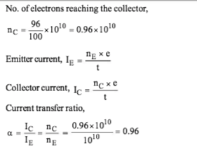
In a npn transistor 1010 electrons enter the emitter in 10–6s. 4% of the electrons are lost in the base. The current transfer ratio will be
-
Solution

In a p-type semiconductor the acceptor level is situated 60meV above the valence band. The maximum wavelength of light required to produce a hole will be
-
Solution

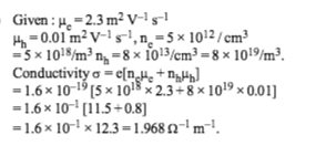
What is the conductivity of a semiconductor if electron density = 5 × 10¹²/cm3 and hole density = 8 × 10¹³/cm3(µe = 2.3 m2 V–1 s–1, µh = 0.01 m2V–1 s–1 )
-
Solution

The gate for which output is high if atleast one input is low?
The current gain of a transistor in common base mode is 0.995. The current gain of the same transistor in common emitter mode is
When the forward bias voltage of a diode is changed from 0.6 V to 0.7 V, the current changes from 5 mA to 15 mA.Then its forward bias resistance is
-
Solution

In a reverse biased diode when the applied voltage changes by 1 V, the current is found to change by 0.5 µA. The reverse bias resistance of the diode is
-
Solution

The intrinsic conductivity of germanium at 27° is 2.13 mho m–1 and mobilities of electrons and holes are 0.38 and 0.18 m2V–1s–1 respectively. The density of charge carriers is
-
Solution

The cause of the potential barrier in a p-n diode is
-
Solution
During the formation of a junction diode, holes from p-region diffuse into n-region and electrons from n-region diffuse into p-region. In both cases, when an electron smeets a hole, they cancel the effect at each other and as a result, a thin layer at the junction becomes free from any of charges carriers. This is called depletion layer.There is a potential gradient in the depletion layer,negative on the p-side,and positive on the n-side. The potential difference thus developed across the junction is called potential barrier.
The truth-table given below is for which gate?

-
Solution
Relation between A, B and C shows that C=\(\overline{AB}\) So NAND Gate


